Aug. 29, 2017
By: Michael Feldman
If there was any question that machine learning would spawn chip designs aimed specifically at those applications, those doubts were laid to rest this year. The last 12 months have seen a veritable of explosion of silicon built for this new application space.
 The first hint that machine learning would not be business as usual for chipmakers was when Google revealed its own Tensor Processor Unit (TPU) ASIC earlier this year. Unbeknownst to Google users, those first-generation TPUs had been in operation since 2015, accelerating searches, language translation, and other machine-learning-accelerated services. While that initial design was aimed at inferencing already trained neural networks, Google’s second-generation TPU, which it announced just six weeks after it had revealed the details of the first chip, was designed for both inferencing and training.
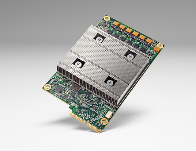
At the same time Google was inserting custom-built chips into its cloud, Microsoft was taking a similar tack with FPGAs. Although the software-maker purchased the FPGAs from Intel (Stratix V and Arria 10), it was essentially turning them into machine learning chips, by configuring them to run inferencing workloads. In this case, the FPGAs were deployed across Microsoft’s Azure cloud to accelerate things like Bing searches, image recognition, and Skype language translation. Last September, the company demonstrated a real-time translation of Wikipedia, which was able to draw on an exaflops worth of Azure-deployed FPGAs. Last week, Microsoft revealed it was now outfitting Azure with the more powerful Stratix 10 FPGAs.
Baidu has also been exploring the idea of using FPGAs programmed for machine learning. In July, Xilinx announced Baidu would deploy its Kintex FPGAs as the basis of a new cloud-based service for third-party deep learning and encryption applications. (Amazon unveiled a similar FPGA-cloud offering last December, also based on Xilinx silicon.) At the Hot Chips conference last week, Baidu revealed it was developing an XPU, a custom-built FPGA-based solution that devotes a portion of its reconfigurable logic to implement a simple manycore CPU. Notably, these FPGA solutions are not hard-coded for machine learning, but without the draw of this application set, it’s unlikely if any of these offerings would have made it out of the research lab.
Returning to the custom-built ASIC approach, we have startups like Graphcore and Wave Computing. Graphcore has branded their solution as the Intelligent Processing Unit (IPU), and according to the company has designed it to run both training and inferencing workloads 50 to 100 times faster than a GPU. Wave Computing, meanwhile, is offering a machine learning appliance based on its custom-built clockless chip, known as the Dataflow Processing Unit (DPU). A 16-DPU appliance can offer 2.9 petaops/second of peak performance.
Fujitsu is developing its own machine learning ASIC, dubbed the Deep Learning Unit (DLU), which will take advantage of the company’s Tofu interconnect technology to support large-scale neural networks. Initially, the company plans to offer the DPU as a coprocessor, but the second-generation product will merge the logic with a CPU to provide a standalone solution.
The elephant in the room is, of course, NVIDIA, which, from the chip provider perspective, currently dominates the machine learning market. Thanks to built-in support for single-precision and half-precision floating point operations, NVIDIA GPUs offer some of the best performance for machine learning applications. Perhaps more importantly, the company’s development of an extensive software ecosystem for machine learning frameworks and application libraries have made their products widely accessible to developers.
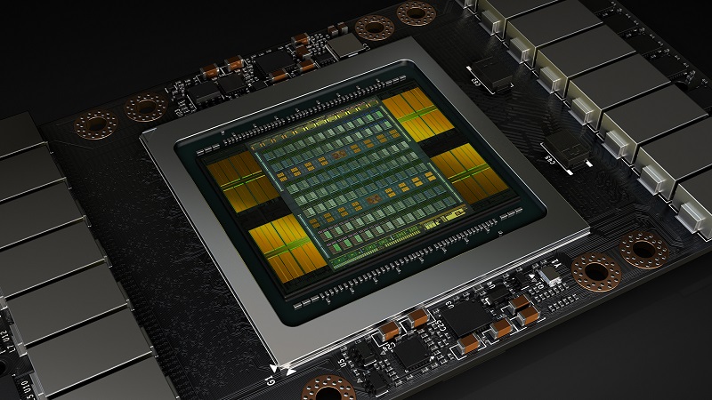 For the most part, NVIDIA accomplished this without the use of custom silicon. We say for the most part, since its latest Volta-class V100 GPU is outfitted with 640 Tensor Cores, which are purpose-built structures that perform the kind of mixed precision matrix math (32-bit and 16-bit floating point) that deep learning codes thrive on. As a result, each V100 can deliver 120 deep learning teraflops. That’s nearly as good as the 180 teraflops delivered by Google’s custom-built TPU, although it’s not clear if the latter is implemented with the same mix of flops.
If the elephant in the room is NVIDIA, the elephant-hunter would be Intel. Its strategy is to use a combination of the Xeon Phi technology and the Nervana-acquired IP to develop purpose-built machine learning chips. The company’s latest reveal of Knights Mill, a Knights Landing variant tweaked for machine learning codes, swaps some of the Xeon Phi’s double precision real estate for more single precision performance and support for lower precision integer math. That chip is schedule for launch later this year, which will presumably be followed by Lake Crest, a deep learning coprocessor derived from Nervana technology. Both are to be used for training deep learning models, so will go head-to-head against NVIDIA’s V100 GPU.
AMD is also challenging NVIDIA in the machine learning area, primarily with its new Radeon Instinct products – initially the MI6, MI8, and MI25 GPUs. Like Knights Mill, the Instinct GPUs jettisoned the double precision transistors in favor of the more targeted single and half precision logic. AMD continues to maintain a distinct Firepro line of GPUs for general-purpose HPC acceleration.
The choice between embedding machine learning logic and capabilities into a more general-purpose design, as NVIDIA has done with its GPUs, or breaking them out into separate chips as Intel, AMD, Fujitsu and others are doing, remains a central question. It worth noting that neither NVIDIA nor Intel are completely devoted to either approach: Intel has built machine learning capabilities into its latest "Skylake" Xeon processors, while NVIDIA has developed an dedicated inferencing unit, known as the Deep Learning Accelerator. Regardless of who's doing what, at this point, there is no consensus about which approach will prevail, and it’s quite possible that both will enjoy viable markets.
An area where custom chips might struggle is HPC itself, where machine learning codes are being inserted into simulation workflows. For example, machine learning can be used to mine intelligence from the simulation’s output data (like weather prediction data), as well as to determine the most useful constraints for those simulations in the first place. In these cases, a system containing processors that can flip between physics and neural network computation would be ideal. Having to deploy and maintain separate infrastructure for these two types of application would likely be more costly, even if performance could be optimized with more customized hardware.
The downside is that integrating machine learning smarts onto a general-purpose chip makes the die bigger and more complex, and thus more expensive. NVIDIA’s V100 die contains a whopping 21 billion transistors, which is about a third larger than the previous-generation P100. Even if die space was not a consideration, the extra real estate employed for the application-specific Tensor Cores on the V100 could have presumably been used to deliver more double precision or single precision performance.
In any case, it’s not a simple formulation. The diversity of machine learning applications and the dichotomy between training and inferencing are going to demand a wide array of solutions. And given that this application space is just beginning, we’re likely to see an even more varied array of designs before any sort of consolidation takes hold. Exciting times.