
Aug. 1, 2018
By: Michael Feldman
The Defense Advanced Research Projects Agency (DARPA) has selected the teams for two research programs that the agency hopes will provide technologies to transcend the limits of Moore’s Law.
 As part of DARPA’s $1.5 billion Electronics Resurgence Initiative (ERI) to “jumpstart innovation in the electronics industry,” the Three Dimensional Monolithic System-on-a-Chip (3DSoC) program and the Foundations Required for Novel Compute (FRANC) program are focused on developing chip-level innovations that lead to more powerful and efficient computing systems. We reported on both programs last September, just after they were announced
Last week, during DARPA’s first ERI Summit in San Francisco, the agency revealed the research teams selected to drive each of these efforts. For the 3DSoC program, groups from the Georgia Institute of Technology, Stanford University, Massachusetts Institute of Technology, and Skywater Technology Foundry were tapped. The corresponding research teams for the FRANC program will come from HRL Laboratories; Applied Materials, Inc.; Ferric, Inc.; the University of California, Los Angeles; the University of Minnesota; and the University of Illinois at Urbana-Champaign.
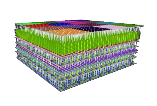
The stated goal of the 3DSoC program is to “develop materials, design tools, and fabrication techniques for building microsystems on a single substrate with a third dimension.” The idea is to be able to construct vertically integrated devices that will include logic and memory, as well as I/O elements. The advantage of doing so is that data transit times between these different components is dramatically reduced, yielding much better overall throughput.
Leading the 3DSoC work is Linton Salmon, a DARPA Microsystems Technology Office program manager. “Under the 3DSoC program, the researchers will build on a decade’s worth of theory and academic demonstration to integrate processes into a widely available foundry that should help, in practice, unleash these technologies in the field of microelectronics,” said Salmon.
Compared to conventional systems built from discrete 2D chips, DARPA thinks the 3DSoC effort can yield more than a 50-fold reduction in computation times, while using just a fraction of the power. To meet these goals, the 3DSoC designs should support an inter-layer interconnect bandwidth of 50 terabits per second and require no more than 2 picojoules per bit to access memory.
The main impetus behind the 3DSoC work is to address the memory limitations of traditional architectures related to bandwidth, latency, and energy consumption. To some degree, this is already being done with current 3D and 2.5D stacked memory devices that are integrated with NVIDIA Tesla and AMD Radeon Instinct GPUs, as well as Xeon Phi processors. But the 3DSoC designs being envisioned are more complex, incorporating a dozen or more layers, and integrating things like resistive random-access memory (ReRAM), carbon nanotube transistors (CNFET), and regular silicon MOSFET-based processor cores.
The researchers at Stanford University have already simulated such 3D dies on 7nm and 90nm process nodes and applied them to various neural network training and inferencing models. The simulations revealed significant benefits – expressed as a product of energy use and execution time – compared to conventional 2D chips at 7nm. For a 7nm 3D SoC, the researchers claimed benefits of between 323x to 646x compared to a 2D chip. Even at 90nm, the simulated 3D SoC delivered 35x to 75x more benefit compared to conventional 7nm 2D devices. Similar results were obtained for a variety of algorithms, including linear regression, logistic regression, PageRank, Single Source Shortest Path (SSSP), and Breadth First Search (BFS).
Closely related to the 3DSoC work is the FRANC program, which is aimed exclusively at the memory-logic bottleneck. Its goal is to “transcend the conventional separation of logic and memory functions in what are known as von Neumann architectures.” In essence, the idea is to process the data where it’s stored, rather than having to move it to where the computing elements reside, lowering energy consumption and improving throughput. The multi-pronged approach will involve developing novel circuit designs and using new materials and integration techniques to minimize data movement.
Y.K. Chen, another Microsystems Technology Office program manager at DARPA, will head the FRANC program. “FRANC seeks to utilize new materials and devices to make 10x advances in embedded, non-volatile memories with the speed of static random access memory (SRAM) and the density of storage-class memory,” said Chen. “These advances could allow emerging memory-centric computing architectures to overcome the memory bottleneck presented in current von Neumann computing.”
FRANC will build from other processing-in-memory and processing-near-memory work, such as DARPA’s own STARnet program, but aims to forge its own path. In particular, it will allow for designs that incorporate accelerators that employ new materials and integration technology. Areas of interest include material discovery, power management, on-chip photonics (for both CMOS and DRAM), and emerging non-volatile memory technologies. Some examples of the latter include Mott memory, carbon memory, molecular memory, and ferroelectric tunnel junctions.
Both the 3DSoC and FRANC programs are mandated to produce tangible results – EDA tools plus 3D chip designs for the 3DSoC work, and a functioning prototype in the case of the FRANC effort. The 3DSoC program is scheduled to last four and a half years, while FRANC has a timeline of three and a half years. With the research teams now in place, work is expected to commence immediately.