July 28, 2016
By: Michael Feldman
AMD has flirted with the idea of building big brawny APUs for servers ever since the company starting developing the CPU-GPU hybrid chips begin back in 2006. Combining x86 and Radeon silicon on the same die for desktops and laptops was the basis for AMD’s original Fusion processor, later renamed as the Accelerated Processing Unit (APU). Now with the anticipation of the next-generation “Zen” CPU core and the future “Vega” GPU, it looks like a high-performance server APU could finally become a reality.
AMD CEO Lisa Su reiterated the goal to build such a processor at the end of last week’s Q2 earnings call. “I think it’s fair to say that we do believe that we can combine a high performance CPU with a high performance GPU,” said Su, adding that “it’s an area where combining the two technologies makes a lot of sense.”
 It’s not like AMD is a stranger to this technology. The company has built less performant APUs for personal computers for some time, and even produced an APU microserver SoC in 2013. That chip, known as the “Kyoto” Opteron X2150, was a quad-core x86 CPU blended with 128 Radeon cores. It drew just 11 watts and became the basis for the HP ConvergedSystem 100, a Moonshot machine aimed at virtual desktop interface (VDI) work.
The microserver business never took off the way many had predicted, but the idea of more powerful APUs endured. AMD custom-built APU-type chips for the Xbox One and PlayStation 4 gaming consoles. Both of those processors housed eight “Jaguar” x86 cores, alongside Radeon cores. Peak single-precision performance for the Xbox One chip was about 1.3 teraflops, while the PS4 processor topped out at 1.8 teraflops.
The first inklings that AMD was serious about an HPC-class APU based on newer CPU and GPU architectures came last year at the company’s Financial Analyst Day, when they openly discussed high-performance APUs for workstations and servers, based on AMD’s Heterogeneous System Architecture (HSA) framework. No specific details or dates were revealed, although the processors were characterized as multi-teraflop platforms, which would integrate a 3D stack of high bandwidth memory (HBM).
HBM is actually key to building viable high-end APUs, since regular DDR memory is generally too slow to feed a big data-hungry GPU, and even GDDR memory is a bottleneck for the larger GPUs. AMD has already used HBM in the dual-GPU FirePro S9300, which is targeted to HPC servers.
A rumor that an HBM-powered APU was in the works was reported on by Fudzilla in March 2015. The chip would combine 16 Zen cores (up to two threads per core) with a large “Greenland” (now “Vega 10”) GPU. The processor would be hooked up to a 16 GB HBM device via a silicon interposer, and deliver 512 GB/second of memory bandwidth to the APU compute units. Four channels of DDR4 memory would also be included, supporting a maximum capacity of 1 TB. Although those specs clearly point it toward HPC and other high-end server work, such a design could be scaled down to AMD’s desktop and laptop markets as well.
The nominal date for this chip would be 2017, which would put it in roughly in the same timeframe as the two other multi-teraflops processors on the market, namely NVIDIA’s “Pascal” P100 GPU and Intel’s “Knights Landing” Xeon Phi CPU. The advantage for the APU is that it avoids both the data communication challenges of the CPU host/GPU coprocessor model of an NVIDIA discrete GPU, and the performance compromise implicit in a standalone throughput processor like Intel’s Knights Landing, which also must serve the role as a single-thread processor when not crunching vectors.
Does a CPU-GPU hybrid represent enough differentiation for a market that already has two clear choices for floating point acceleration? The US Department of Energy seems to think so. In 2014, they awarded $32 million to AMD to develop its APU technology for exascale computing. The DOE awards were made under the agency’s FastForward 2 program, which split its AMD funding into two areas: one for the server node architecture based on APUs, and the other on advanced memory technology, including new memory interfaces, non-volatile devices, and processing-in-memory designs.
A subsequent IEEE report authored by the AMD’s FastForward principle investigators and others at the company, described the research in some detail. As described, the EHP would combine a CPU and GPU, the latter providing most of the FLOPS. Each APU would provide at least 10 peak teraflops of compute, which would require a system with 100,000 such processors to reach a peak exaflop.
The researchers outlined the advantages of the hybrid architecture, specifically the practicality of offering high single thread performance on the CPU cores and high throughput performance on the GPU cores. Significantly, the CPU and GPU, by virtue of their integration, can share a common memory space, making data access and transfers between the two highly efficient. The power savings in data communications, they believe, gives the APU design a key advantage for exascale.
Not surprisingly, the EHP would also integrate 3D memory. The authors project that for the exascale timeframe, 3D memory such as HBM will be able to provide the needed 4 TB/second of bandwidth, but the per node memory capacity of 1 TB would not be feasible. Instead, they suggest a second tier made up of non-volatile memory (NVM). Interestingly, the researchers believe the NVM will likely be based on emerging technologies such as phase change memory or memristors, rather than DRAM.
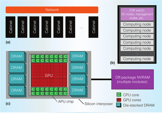 Image: EHP system. Credit: IEEE.
Assuming the EHP design makes it to production, the first chips are not likely to be seen before the turn of the decade. In the interim, if AMD is going to make a play for the HPC market with an APU design, it best do as soon as possible before NVIDIA and Intel lock down the market.
AMD’s discrete GPU FirePro line has not been competitive against NVIDIA’s more established Tesla GPUs or Intel’s Xeon Phi, not because of any significant performance disadvantages, but rather because AMD did not establish its HSA and OpenCL software for its products in the way NVIDIA did for CUDA and Intel did with its x86 software toolset, compilers, and libraries.
With a differentiated product in the APU, AMD could reset its aspirations to be a provider of HPC accelerators, and down the line, exascale supercomputers. The chip could also be used to work its way into deep learning, another market the company let its rivals exploit. For AMD, the question is always focus and execution. Time will tell if Lisa Su and company are really interested in playing in the upper echelons of the server space and are willing to devote the necessary resources to make that happen.