
Aug. 1, 2016
By: Michael Feldman
A new report put out by a consortium of semiconductor industry groups is predicting that Moore’s Law will be renewed in the next decade by transitioning from CMOS technology to something called “3D Power Scaling.” The transition will rely on developing a new breed of low-power transistors that can be manufactured into three-dimensional structures. According to the report, the technology could even accelerate the cadence of Moore’s Law beyond its nominal 2x-per-2-year rhythm.
![]() The basic idea behind this new technology is to increase device densities not by shrinking transistor geometries via the continual refinement of lithographic techniques, but rather by shifting semiconductor manufacturing from 2D to 3D, while also employing new kinds of transistors that are more energy-efficient than those based on conventional CMOS. The post-CMOS low-power transistor technologies are separable from the 3D approach, which we’ll address first.
The basic idea behind this new technology is to increase device densities not by shrinking transistor geometries via the continual refinement of lithographic techniques, but rather by shifting semiconductor manufacturing from 2D to 3D, while also employing new kinds of transistors that are more energy-efficient than those based on conventional CMOS. The post-CMOS low-power transistor technologies are separable from the 3D approach, which we’ll address first.
Building devices in three dimensions is an obvious choice considering the fact that as transistor features approach the 10nm range, leakage current become increasingly problematic. “By 2020-2025, device features will be reduced to a few nanometers and it will become practically impossible to reduce device dimensions any further,” write the report’s authors. While the leakage problem will ultimately lead to the end of transistor shrinkage, employing the third dimension will preserve the Moore’s Law concept of increasing transistor density per area, and do so in a way that maintains the cost and performance advantages inherent in constructing a monolithic device.
3D Power Scaling is very different from the way 3D semiconductor packages are built today. The latter approach relies on stacking multiple 2D dies into three-dimensional packages, using through-silicon vias (TSVs) to integrate the individual devices. This technology is being used being used to construct 3D image sensors and 3D DRAM packages like the Hybrid Memory Cube (HMC) and High Bandwidth Memory (HBM). Challenges include aligning the layers correctly and dealing with the added cost associated with constructing a device from multiple dies. Using 3D Power Scaling avoids those pitfalls since the transistors are vertically oriented and laid down on top of each in a single manufacturing process.
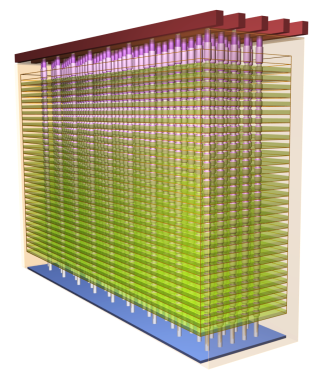 Such technology is already being employed to create 3D NAND flash. NAND technology has already become extremely difficult to scale below 20nm or so, and now requires heroic error correction schemes to deal with endurance and data corruption issues. The initial 3D chips from Micron, Intel, Toshiba, and Samsung use 32 to 64 vertical layers, and are able to produce devices that can store half a terabit. From these, a standard SSD flash drive can be constructed with up to 10 TB of storage, and probably more. Devices with 100 layers and 1 terabit of storage are already on the drawing board. Flash producers are promising not just denser, higher capacity products, but ones that are less expensive.
Image: 32-layer 3D NAND. Credit: Micron Technology
Such a development foreshadows what the ITRS authors believe will happen more generally in the industry in the next decade, eventually extending to all semiconductor devices, including processors. According to a related report from IEEE’s Rebooting Computing initiative, the ability to mix and match transistor types in 3D configurations has another big advantage:
In the 3D Power scaling approach, a logic block could have memory, registers and other related circuits stacked in the planes immediately above and below. This would greatly reduce the distance interconnect lines have to travel and also their cross section could be greatly increase with consequent reduction in signal propagation delay.
Such a configuration would lend itself very well to processor-in-memory (PIM) devices, heterogeneous processors, and on-chip memory hierarchies. All of these designs are possible now, of course, but with planar devices, scalability is naturally limited by the size of the individual die.
The second piece of 3D Power Scaling has to do with its middle name. The ITRS report calls for ditching traditional CMOS in favor of low-power transistor technologies such as tunnel field-effect transistors (TFET) and spin transistors. TFETs can operate at significantly lower voltages than CMOS transistors, and exhibit very little leakage current. Spin transistors rely on the electron’s spin (up or down) to represent its state, and can operate with little electrical current. The technology is particularly suited to non-volatile solid state storage. Both TFET and spin transistors are in the research stage, but the ITRS authors note that progress is being made in both these areas and “their introduction into manufacturing appears consistent with the advent of the next decade.”
One possible limitation would be excessive heat production, since the 3D structures offers less surface area for a given amount of power. The use of lower power transistors will ameliorate this problem to some extent, but as the number of vertical layers grow, the devices will require some external (or perhaps internal) cooling mechanism.
Although the ITRS report cautiously avoided making any quantitative predictions about how semiconductor costs and performance would fair with under 3D Power Scaling, the authors are optimistic that the inherent scalability of using the third dimension will “accelerate the level of transistor density beyond Moore’s Law traditional trend.” Given that practically every industry in the world is now driven by digital technology, that would be good news indeed.