
Aug. 22, 2016
By: Michael Feldman
At the Hot Chips symposium taking place in Cupertino, California this week, Samsung and SK hynix touted their latest efforts for high bandwidth memory (HBM), including the third iteration of the technology, known as HBM3. This new version promises to double bandwidth and density, while taking more direct aim at the high performance computing market.
HBM employs a 3D array of memory chips, stacked vertically and connected in parallel using thru silicon vias (TSVs). Parallelizing the connections between the memory chips has the effect of greatly increasing the bandwidth since the TSVs allow for a much wider memory bus – in the case of HBM, 1024 bits per package, which is eight times wider than GDDR memory. Because of its 3D construction, it is also much denser than that of conventional 2D memory. Plus, it offers greatly improved energy efficiencies. The only thing keeping DDR and GDDR DIMMs in the game at this point is that they are cheaper from a capacity standpoint. And given the intricacies of stacking multiple chips with TSVs, that is going to remain true for some time.
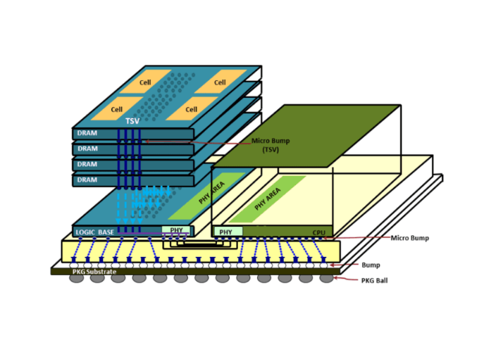
To date, HBM has made its most notable in-roads in replacing graphics memory (GDDR technology) in high-end GPUs from NVIDIA and AMD. It’s main advantage here is keeping these big, brawny chips fed with data and do so within a reasonable power envelope. For the second-generation HBM2 technology, a single 8-stack package of 8Gb chips can deliver 256 GB/sec of bandwidth.
For HPC and deep learning applications, the technology has been integrated into NVIDIA’s Pascal P100 and AMD’s FirePro S9300 x2 processors. In the case of the P100, HBM2 memory is being used, while the dual-GPU FirePro S9300 part uses the original HBM technology. In both cases though, memory bandwidth is greatly improved compared to GDDR technology. Using multiple memory stacks in the processor package, the P100 is able to achieve 720 GB/sec, while the S9300 x2 can hit 1024 GB/sec (each GPU gets 512 GB/sec). That’s considerably faster than any GDDR5 (or DDR4) setup in commercial use today.
During the Hot Chips event, Samsung and SK hynix talked about their future HMC roadmap, which in both cases involved a third iteration of the technology. Dubbed HBM3, it will more than double the bandwidth of HBM2 to 512 GB/sec or more per memory stack. Apparently Samsung is looking to do this by manufacturing memory chips that are at least twice as dense (16Gb or more), and stacking them higher (more than 8). Samsung intends to use lower voltages to keep power consumption on par with that of the previous generation. The first HBM3 product are not expected until the 2019-2020 timeframe. SK hynix had little to say about the particulars of HBM3, except the it would enable the technology to penetrate deeper into applications that its HBM2 products are already targeting, in particular, HPC, graphics, and networking. The memory-maker is looking at applications for both servers and clients.
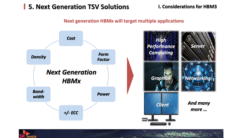
A key to the latter space would be a lower-cost HBM, which just happens to be something Samsung talked the most about at Hot Chips. Specifically, the company is envisioning a device that delivers slightly less performance than HBM2 (around 200 GB/sec per memory stack) and no error correction, but at a fraction of the cost of HBM2 devices. Samsung is not saying how big or small that fraction might be.
While HPC users have no direct interest in a lower cost, less performant HBM aimed at client devices, it could turn out to be the key to the future of this technology. If Samsung could provide HBM products for a volume market like smartphones, that would likely have a very significant effect upstream at the server end of the market. So instead of 3D memory being restricted to pricy accelerators, high-end gaming chips, and specialized networking gear, it could become a component of general-purpose processors that would end up in every server on the planet.
Such an eventuality is conceivable even if Samsung isn’t the company that ends up driving it. The prospects of higher performance, density and energy efficiency will help push the technology toward better price-performance across the client-server landscape. Until actual 3D transistors for RAM become a reality (as they are starting to be in NAND), 3D devices with stacked memory chips looks like the only practical way to overcome the diminishing returns of each succeeding DDR and GDDR generation
Here it’s worth pointing out that Intel and Micron were actually first movers in 3D memory, with their hybrid memory cube (HMC) technology, which they introduced in 2011. HMC operates by similar means as HBM and is aimed at similar purposes. (A version of the technology known as MCDRAM is integrated into Intel’s newest Xeon Phi, known as Knights Landing.) Like its HBM cousin, HMC is currently in its second generation. And it’s almost certain that, like Samsung and SK hynix, Intel and Micron are looking for a way to drive 3D memory into the client space.
Although Micron’s Thomas Pawlowski spoke about HMC at Hot Chips, he had very little to say about the its roadmap. A third-generation HMC standard (3.0) is supposedly in the pipeline and going to be released sometime this year, but he chose not to provide any update on that front. However, Pawlowski couldn’t resist taking a shot at HBM, and by association its competitors Samsung and SK hynix, touting the superiority of the HMC technology over its 3D rival.
In the short-term, the availability of two 3D memory standards is going to cause some confusion in the marketplace as vendors and users choose sides. It would be tempting to say that eventually only one will remain, but given the longevity of the GDDR-DDR dichotomy and the increasing diversity of memory technologies in general, both HBM and HMC may enjoy long and fruitful lives in parallel. For the time being, the competition appears to be driving innovation in both camps, and with that, hopefully better price-performance.