Aug. 24, 2018
By: Michael Feldman
At the Hot Chips conference this week, IBM outlined its plans to develop a new open standard memory interface that would be able to talk to different types of memory devices besides just DDR.
 Those plans were announced as part of a larger presentation at Hot Chips on IBM’s new Power9 scale up processor. This is the same chip used in the recently-announced E980 enterprise server, which allows for up to 16 sockets (192 cores), 64 TB of memory, and 32 PCIe Gen4 x16 slots. The product is geared for industrial-strength database processing and other workloads needing a lot of compute threads, memory, and/or I/O.
In general, these servers are way too expensive for the type of scale-out cluster you see in HPC shops, although they could be used as fat memory nodes in such a setup. For HPC and more mainstream enterprise use, IBM offer’s the scale out Power9, which is built for two-socket servers, such as the IBM AC922. This is one used in the Summit supercomputer.
One of the biggest differences between the two Power9 chips is their memory interface. The scale up version offers better memory bandwidth than its scale out sibling: 230 GB/sec vs 150 GB/sec, as well as more memory capacity per socket: 8 TB vs 2 TB. To do this, the scale up chip uses SerDes links rather than a direct connection to DDR memory. The SerDes links are managed by IBM’s on-chip Differential Memory Interface (DMI) interface, which then talks to IBM’s Centaur memory buffer chips. It’s the buffer chips that are connected to the DDR DIMMs
The memory buffering adds about 10ns of latency to memory accesses compared to a direct DDR hookup, but the tradeoff for more bandwidth and capacity is worth it for these extra-fat servers. And although the Centaur buffered memory implementation still uses DDR memory chips as the storage media, this no longer really needs to be the case since the DDR smarts have moved off the chip.
IBM plans to generalize this memory interface, which will be known as OpenCAPI memory, in their next version of the Power9 processor that is scheduled to be launched in 2019. As far as we can tell, these upcoming Power9 chips will be suitable for two-socket HPC servers, as well as mainstream systems. IBM is projecting that its next Power9 chip will support over 350 GB/sec of memory bandwidth per socket, which is more than twice the speed of today’s fastest chips for two-socket servers. The company also intends to reduce the latency penalty to around 5ns in its first go-around.
Perhaps the bigger news here is that OpenCAPI memory will be proposed as an open standard for the entire industry. The use of the OpenCAPI brand is intentional, since IBM wants to do for memory devices, what the original OpenCAPI was designed to do for I/O devices, namely level the playing field. In this case, the idea is to enable any processor to talk to any type of memory via conventional SerDes links. As a result, CPUs, GPUs, or FPGAs would no longer need to be locked into DDR, GDDR, or any other type of memory technology. So, for example, a chip could use the interface to connect to traditional DDR-type DIMMs, storage-class memory based on NAND or 3D XPoint, or some other type of specialized memory.
Of course, establishing a new standard is no easy feat, especially when it comes to entrenched technologies like DDR. Assuming this all goes as planned, it will be interesting to see who signs on to OpenCAPI memory when it’s launched next year. Beyond that, we can expect IBM to reveal more details on the next-generation Power9 processor as we get closer to its 2019 launch date.
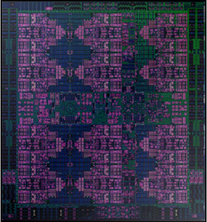
Image: Power9 Scale Up Processor. Source: IBM