Oct. 5, 2016
By: Michael Feldman
This week, Adapteva CEO Andreas Olofsson announced his company has taped out the Epiphany-V, a 1024-core RISC chip that will likely offer the world’s best performance per watt for double precision arithmetic. This SoC is geared for high performance computing (HPC) in applications such as self-driving cars, autonomous drones and cognitive radio, where performance-per-watt is the most critical attribute.
The Epiphany-V design was developed with funding help from DARPA – the Defense Advanced Research Projects Agency. As the research arm for the US Department of Defense, DARPA is intensely interested in advancing low-power, high performance hardware for a wide range of military and security uses. Although the emphasis here is on embedded computing, there’s nothing to prevent some enterprising HPC vendor from building a supercomputing server with a bunch of Epiphany V chips.
According Olofsson’s report on the Epiphany-V, the goal of the design was to demonstrate an energy efficiency of 75 double precision gigaflops/watt. For those of you keeping score, that’s about four times the efficiency of NVIDIA’s new P100 GPU and more than five time that of Intel’s Knights Landing Xeon Phi. Olofsson also claims the chip has an 80-fold advantage in processor density and a 3.6-fold advantage in memory density compared to “the leading HPC processors.”
That’s quite a feat given that the 4.5 billion-transistor chip is manufactured with the same technology NVIDIA uses for their latest Pascal GPUs, namely TSMC’s 16nm FinFET process. Epiphany-V differs from its 64-core Epiphany-IV predecessor in a number of important ways. To start with, it’s the first Adapteva design to support double precision floating point math, which is a requirement for many HPC codes. In addition, the RISC processing elements are capable of hosting an OS, something that the previous version was incapable of doing. That makes it more like an Intel Xeon Phi than a GPU accelerator.
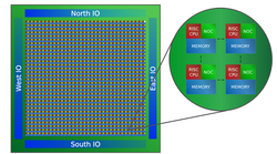
 Source: Adapteva
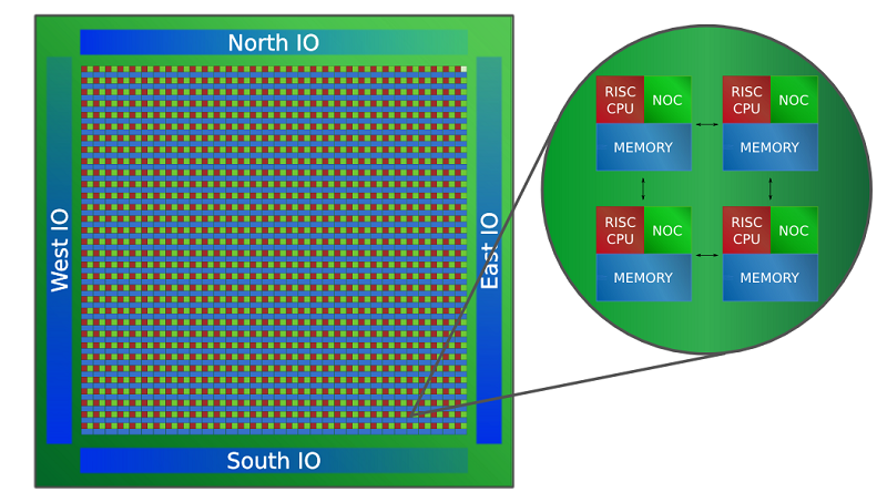
Each of the 1024 “processors” is made up of a RISC CPU, a network-on-a-chip component, and local SRAM memory. There is no cache to speak of. Memory is provided by the 64 MB of SRAM, which can be shared between multiple chips via point-to-point I/O links. Apparently up to a billion cores can be hooked together in this manner, all accessing a global shared memory pool, which can range up to a petabyte of capacity. The individual processing elements on the chip talk to each other over a 136-bit wide data link on the NOCs.
The biggest roadblock to customer adoption is the proprietary instruction set architecture (ISA) than underlies the hardware. (The latest ISA is backwardly compatible with the previous two renditions of Epiphany, with some new instructions added for deep learning, communication, and cryptography applications.) A stable ecosystem of compilers, debuggers and other software development tools will be needed to get customers to consider such an architecture. As of today, the chip can be programmed in ANSI C/C++ using a standard GNU tool chain. Support for MPI, OpenMP, OpenCL, OpenSHMEM and a few other HPC frameworks is also available.
Although Olofsson says the first Epiphany-V chips aren’t expected to roll out of TSMC’s fabs for another four to five months, he expects the new silicon to beat the stated performance goals. "Based on simulations, we will likely exceed 75 gigaflops/watt,” Olofsson told TOP500 News, “but we won't know for sure until we fully characterize the silicon in a few months’ time."